24/2/2022
Today, vias are an integral part of any electronic board sold in the world. Progressively more present and gradually more complex, they allow the very existence of certain highly technical components such as BGAs.
A real
know-how that spreads over two families of vias:
- Mechanical vias
- Laser vias
MECHANICAL VIAS
Mechanical vias are themselves separated into 4 categories namely through vias (1), buried vias (2), backdrilling vias (3) and blind vias, an equivalent to microvias which will be discussed later (4).
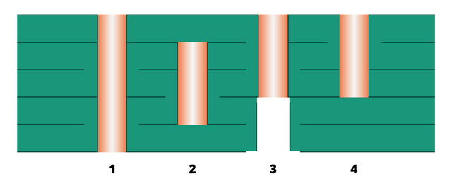
The most
basic via, and therefore the most common and least expensive, is the through
via. Made by drilling with a simple drill and then plating, it is highly
dependent on the quality of the tooling. A few rules must be observed when
designing the routing:
- Observe a ratio of 1/12 between the total thickness of the PCB and the diameter of the drilling tool, this value may depend on the capabilities of the PCB manufacturer.
- Observe a distance of 0.35 mm between two adjacent holes (remaining material thickness).
- Taking into account the thickness of the metallization, the drilling should be done with the following rule: Hole diameter = finished hole diameter (CAD diameter) + 0.1 mm
- Apply the minimum track width values to the copper rings of the vias taking into account the hole diameter.
Example: 0.3 mm pad, 0.15 mm finished hole. The drilling will be done with a 0.25mm tool, the residual copper ring before plating will be 25 µm. This via is not manufacturable.
Today, there is also an increasingly standard option: vias plugging. This technique makes it possible to use vias in Pad, thus allowing the densification of the boards by avoiding having the surface of the vias preventing the installation of components. Moreover, it allows the use of certain fine pitch components without the need for laser vias and finally their last uses are for the creation of thermal vias on the power pad of components.
The technology proposed by EMSFACTORY is called "Filled and Capped". The vias are capped with resin and then the surface is remetallized according to IPC-4761 Type VII.
LASER VIAS
There are vias that are increasingly used, particularly in the context of high density cards, called laser vias. These vias have allowed the appearance of microvias with a diameter of 100µm or less. They include blind vias (1), staggered vias (2(a) and 2(b)) and stacked vias (3)
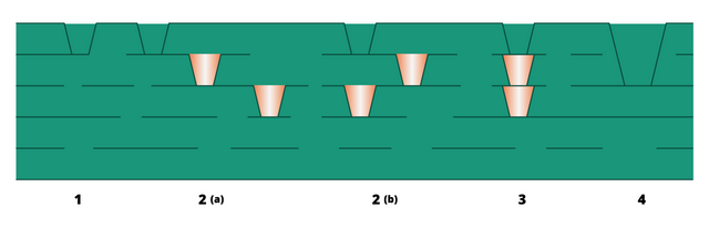
Laser
drilling does not allow very deep holes to be drilled: max. 110µm due to the
laser cone phenomenon (4). The laser drilling method is a very efficient way of
drilling into the prepreg material and thus producing multi-layer circuits with
thin layers.
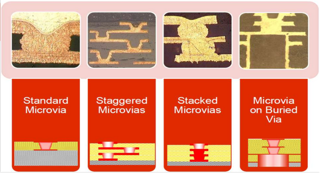
There are
also multiple variants combining these various methods, allowing for use in all
possible PCB configurations with standard or non-standard stackups.
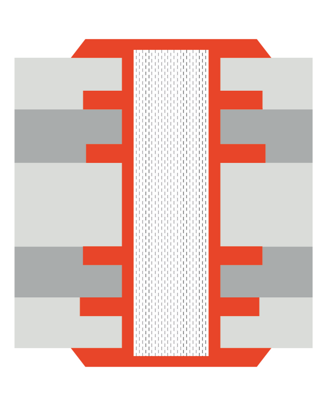
Here is a cutaway from our partner Würth Elektronik to illustrate the point:
Vias,
although central to PCB design, are often neglected and poorly suited to the
purpose for which they were created. Correctly placed, they can also contribute
to the "shielding" of RF signals, to the uniformity of certain
voltages and many others.
Don't hesitate
to contact EMSFACTORY's technical teams who are here to provide you with their
support and knowledge in PCB, industrialization and PCB Design.
Ultimi articoli


Hai bisogno di assistenza?

FAQ

Risorse
